Hamid Abbasi*
University of Mazandaran, Iran.
*Corresponding Author: Hamid Abbasi, University of Mazandaran, Iran.
Received: 27 September 2023; Accepted: 18 October 2023; Published: 00 October 2023.
Using two metal insulated metal waveguides (MIM) and five resonator (a quadrilateral cavity and three rings with different dimensions), we design a plasmonic refractive index sensor. Using the time domain finite difference method, we examine and analyze the sensor performance (numerical analysis) and using the transmission line model method, we theoretically examine the performance of the sensor By summarizing these two methods and calculating the sensitivity coefficient S, quality coefficient Q and figure of merit (FOM), a plasmonic sensor with good performance is obtained. Using the supermods of the resonators, we will achieve a stable wavelength spectrum and a suitable and stable sensitivity coefficient spectrum. Challenges and changes that occur in different modes of this sensor will lead to a balanced and relatively good structure. This designed sensor can be useful in the development of integrated optical circuits.
plasmonics, Surface plasmon polaritons, Metal-Insulator Metal, refractive index sensor.
1. Introduction:
The polariton surface plasmons has been noted for their ability to modulate light at the nanoscale as well as to refract diffraction. SP waves are a longitudinal charge density distribution generated on the metal side interface when light propagates through the metal. When plasmon is excited at this common surface, the fields are strongly enclosed at this surface and decompose rapidly on both sides of the metal and dielectric. Both metal and dielectric specimens can have complex refractive indices of ?m = √nm and ?d = √ , respectively. Within the electrodynamics approach, the surface plasmon propagates as an electromagnetic wave parallel to the x direction with magnetic field oriented parallel to the y direction, that is, transverse magnetic polarization (TM or P) state. The condition of (TM) polarization state is needed to generate the charge distribution on the metal interface, which is considered as the first condition for SP excitation. The SP phenomenon can be easily understood, and its main characteristics can be determined by solving Maxwell’s equation to the boundary-value problem [1,2]. One of the most important tools that can use SP waves to develop integrated optical circuits is the plasmonic sensor. Plasmonic sensors are more suitable for integration due to their very small size and show stronger sensing performance [3]. Recently, various types of plasmonic sensors have appeared, such refractive index sensors [4], temperature sensors [5], phase sensors [6] and gas sensors [7]. The metal-insulator-metal (MIM) waveguide is one of the basic plasmonic waveguides with the capability to confine light within considerable propagating length [8] and many works of sensor are based on this structure [9-17]. Parameters such as high transmission efficiency, high resolution, high quality factor, optical stability, adjustable range of wavelengths, sensitivity (S) and figure of merit (FOM), should be considered in the structure of plasmonic sensors for excellent performance sensor with Provide high optical resolution. In this study, arrays of metal-insulated-metal plasmon waveguides and resonators are designed and simulated to design and fabricate plasmonic sensors. The purpose of this work is to achieve the desired parameters in plasmonic sensors and its development in optically integrated circuits [18].
2. Structural model and theory analysis
The two-dimensional schematic view of the proposed plasmonic refractive index sensor consists of a quadrilateral cavity resonator and three rings with different dimensions along with two input and output waveguides are shown in Figure 1.
The structure of the sensor consists of two plasmonic waveguides with a height of w1 = 50 nm and a quadrilateral cavity with a height of w2 = 270 nm and a length of L1 = 200 nm and three rings. The upper ring at the top of the cavity has an inner radius of r1 = 62 nm and an outer radius of R1 = 92 nm. The two nested rings at the bottom have an inner radius of r2 = 100 nm and r3 = 62 nm and an outer radius of R2 = 149 nm and R3 = 62 nm, respectively.
Pin and Pout monitors are used to measure input and output. The transfer rate is calculated by the following equation:
T = Pout / Pin (1)
Dimensions are optimized for better performance of the sensor structure in the near-infrared region.
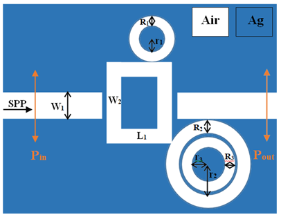
Figure 1: Two-dimensional image of a plasmonic sensor.
3. Limited difference time domain method and transmission line model
Using the time domain finite difference method, we examine and analyze the sensor performance (numerical analysis) and using the transmission line model method, we theoretically examine the performance of the sensor. Summarizing these two methods, we analyze the proposed structure resonance behavior and get a sensor with good performance is obtained [19-21].
The mesh size for the x and y directions of the structure is 8 and 8 nm, respectively. Most plasmonic devices proposed and designed to test the performance of devices with much shorter simulation time and less drop use two-dimensional simulation.
To show the optical properties of metals in simulation, we use the drude model. For practical purposes, a major advantage of the Droud model is that it can be easily incorporated into Maxwell equations in time-based numerical solutions (such as finite-time finite difference method):

Here c∞ =1 gives the medium constant for the infinite frequency, ωp = 1.37 × 10¹⁶ refers to bulk frequency for plasma, γ = 3.21 × 10¹³ means damping frequency for electron oscillation, and ω shows incident light angular frequency.
The TM wave starts moving from the left and is used for SPP excited waves and is published in the waveguideand the closer it gets to the output port, the less intense it becomes.
Each resonator reflects a portion of the input signal. As shown in Figure 2, the intermediate cavity absorbs the largest amount of TM wave and also has the highest field exchange with waveguides, thus having a greater impact on sensor performance.
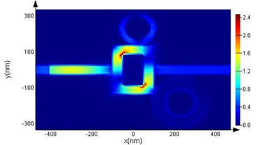
Figure 2: Electric field distribution at resonant frequency
When the field distribution in the sensor structure is similar, energy loss is reduced. To achieve the maximum field distribution in the simulated structure, all dimensions must be optimized. Therefore, we plot the structure transfer spectrum (Figure 3).
First, we draw the transmission spectrum for a quadrilateral cavity. In the next step, we add the upper ring (R1) and then we add the bottom ring (R2) and in the last step, we add the bottom nested ring (R3).
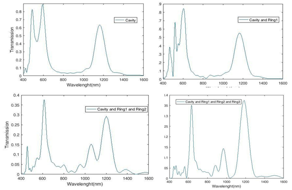
Figure 3: The transmission spectra of MIM waveguide coupled with a cavity and three rings R1 and R2 and R3
The most suitable structure in the transmission spectra is formed when the cavity and the three rings are present at the same time. We now increase the dielectric refractive index by 0.01 nm from 1.11 to 1.2, which changes the spectra and resonant wavelengths. We see the transmission spectrum resulting from the change of the sensor refractive index in Figure 4.
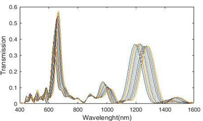
Figure 4: Plasmonic refractive index sensor transmission spectra
To measure the performance of a plasmonic sensor, we need to consider several criteria. The first criterion is the sensitivity S, which is described as the change in resonance wavelength when the dielectric changes unit:
S = Δλ / Δn (nm / RIU) (3)
In this equation, Δλ is the resonance wavelength change and Δn is the refractive index change. We see the sensitivity coefficient diagram of the plasmonic sensor in Figure 5. According to the figure, the maximum sensitivity for the refractive index is n = 1.19 (mode2), which is equal to 1510 nm / RIU. According to this diagram, there is a relatively linear relationship between the two parameters of resonance wavelength and refractive index.
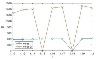
Figure 5: Plasmonic sensor sensitivity coefficient diagram
The next criterion is the figure of merit (FOM) whose equation is as follows:
FOM = S / FWHM (4)
The figure of merit (FOM) for the plasmonic sensor is plotted in Figure 6. According to the figure, the maximum figure of merit (FOM) for the refractive index is n = 1.19 (in mode2), which is equal to 13.617 nm / RIU.
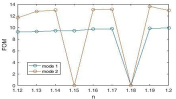
Figure 6: Plasmonic sensor figure of merit (FOM)
The last criterion is the quality factor Q, which is obtained according to Equation 5:
Q = λres / FWHM (5)
We see the diagram of the quality coefficient of the plasmonic sensor in Figure 7. According to the figure, the highest quality factor Q is for the refractive index n = 1.19 (in mode1), which is equal to 15.87 nm / RIU.
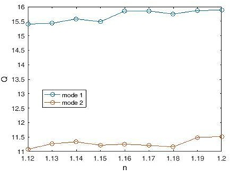
Figure 7: Plasmonic sensor quality coefficient diagram
Equations 3, 4 and 5 have evaluated the sensing capabilities of plasmon sensors and we conclude that this sensor has an optimal structure and has a high sensitivity.
Conclusion:
An amplifier system connected to a plasmonic waveguide, consisting of a metal-insulated metal waveguide (MIM) with a cavity and three rings, has been designed and numerically evaluated using the time-difference method. The two resonance peaks have different dependencies on the structural parameters due to different mechanisms and are easily adjustable. In addition, due to its high resolution resolution, this sensor can easily detect a change in refractive index of 0.01 for materials with a refractive index of between 1.11 and 1.2. The maximum refractive index sensitivity of the proposed structure is 1510 nm / RIU. The proposed structure is expected to provide guidelines for the design of nano-sensors.
Disclosures:
The authors declare no conflicts of interest.
Competing Interest:
The authors declare that they have no competing interests.
Data availability.
The data that support the findings of this study are available from the corresponding author upon reasonable request.
References
- Sabine Szunerits, Rabah Boukherroub. Introduction to Plasmonics: Advancesand Applications (2015).
- Ebbesen, Thomas W, A Dereux, et al. Barnes. Surface plasmon subwavelength optics. Nature 424 (2003): 824-830.
- Tong, L. Recent advances in plasmonic sensors. Sensors 14 (2014): 7959.
- Y Shen, JH Zhou, TR Liu, et al. Plasmonic gold mushroom arrays with refractive index sensing figures of merit approaching the theoretical limit. Nat. Commun 4 (2013): 2381.
- Srivastava, Triranjita, R Das, et al. Highly Sensitive Plasmonic Temperature Sensor Based on Photonic Crystal Surface Plasmon Waveguide. Plasmonics 8 (2013): 515-521.
- Maisonneuve M. Phase sensitive sensor on plasmonic nanograting structures. Optics Express 19 (2011): 26318-26324.
- Elsayed, Mohamed Y, Y Ismail, et al. Semiconductor plasmonic gas sensor using on-chip infrared spectroscopy. Applied Physics 123 (2017): 113.
- Maier, Stefan A. Plasmonics: Fundamentals and Applications. Springer Berlin 52 (2014): 49-74.
- Shu, Changgan. The sensing characteristics of plasmonic waveguide with a ring resonator. Optics Express 22 (2014): 7669-7677.
- Yan, Shu Bin. A Refractive Index Sensor Based on a Metal-Insulator-Metal Waveguide-Coupled Ring Resonator. Sensors 15 (2015): 29183-29191.
- Huang, Ye Xiong. A plasmonic refractive index sensor based on a MIM waveguide with a side- coupled nanodisk resonator. IEEE, International Conference on Embedded and Real-Time Computing Systems and Applications IEEE (2014): 1-5.
- Wu, Tiesheng. A nanometeric temperature sensor based on plasmonic waveguide with an ethanol- sealed rectangular cavity. Optics Communications 339 (2015): 1-6.
- Tang Y. Refractive Index Sensor Based on Fano Resonances in Metal-Insulator-Metal Waveguides Coupled with Resonators. Sensors 17 (2017): 784.
- Zhang, Zhidong. Fano Resonance Based on Metal-Insulator-Metal Waveguide-Coupled Double Rectangular Cavities for Plasmonic Nanosensors. Sensors 16 (2016): 642.
- Zafar, Rukhsar, and M. Salim. Enhanced Figure of Merit in Fano Resonance-Based Plasmonic Refractive Index Sensor. IEEE Sensors Journal 15 (2015): 6313-6317.
- Chen, Jianjun. Coupled-Resonator-Induced Fano Resonances for Plasmonic Sensing with Ultra- High Figure of Merits. Plasmonics 8 (2013): 1627-1631.
- Zhao X, Z Zhang and S. Yan. Tunable Fano Resonance in Asymmetric MIM Waveguide Structure. Sensors 17 (2017): 1494.
- Zhaojian Zhang, Junbo Yang, Xin He, et al. Plasmonic Refractive Index Sensor with High Figure of Merit Based on Concentric-Rings Resonator Sensors (Basel) 18 (2018): 116.
- Allen Taflove, Susan C Hagness. Computational Electrodynamics: The Finite-difference Time-domain Method (2005).
- J Gierak, A Madouri, AL Biance, et al. “Sub-5 nm FIB direct patterning of nano devices,” Microelectron. Eng 84 (2007): 779–783.
- W Wu, J Yang, J Zhang, et al. “Ultra high resolution filter and optical field modulator based on a surface plasmon polariton,” Opt. Lett 41 (2016): 2310–2313.